
In the manufacturing of high - end HDI boards, the timing coordination and process connection logic between laser drilling and back drilling in multi - layer lamination are crucial. Laser drilling is usually carried out in the early stage of the process, creating precise 0.1mm blind holes. These blind holes play a vital role in the electrical connection of the board. After laser drilling, back drilling with a diameter of 0.5mm comes into play. The back drilling process needs to be precisely coordinated with the previous laser drilling, ensuring that the holes are properly aligned and the electrical performance of the board is not affected. For example, if the back drilling is carried out too early, it may damage the blind holes created by laser drilling; if it is too late, it may lead to problems in the overall assembly process.
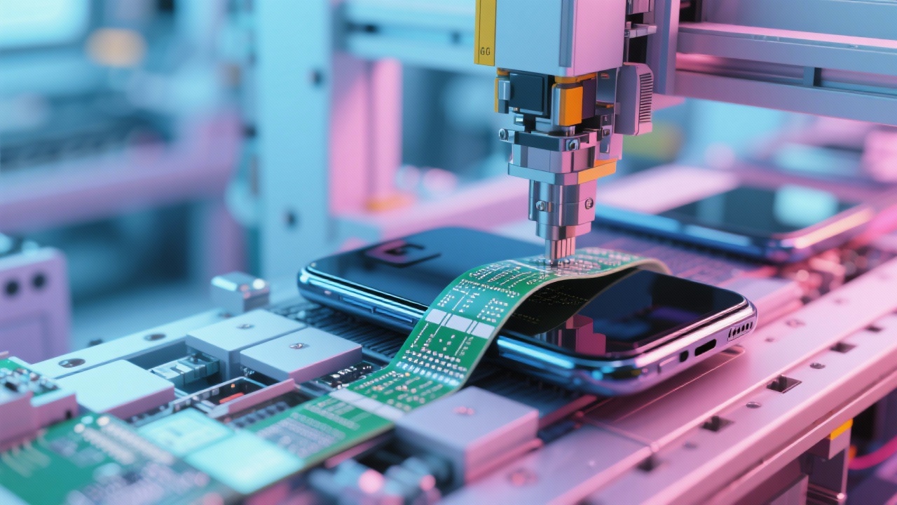
One of the core challenges in high - end HDI board manufacturing is the size matching between 0.1mm blind holes and 0.5mm back - drilled holes. A small deviation in size can lead to electrical connection problems, such as short - circuits or open - circuits. To ensure size accuracy, manufacturers need to use advanced measurement and control systems. For instance, high - precision optical measurement devices can be used to measure the diameter and position of the holes in real - time during the manufacturing process, and adjust the drilling parameters accordingly.
The consistency of hole wall plating is another significant issue. Uneven plating can cause differences in electrical conductivity, affecting the overall performance of the board. Factors such as plating solution composition, plating time, and temperature need to be strictly controlled. For example, maintaining a stable plating solution temperature within a range of ±1°C can significantly improve the plating consistency.
Inter - layer offset can lead to misalignment of electrical connections, which is a major problem in multi - layer HDI boards. Advanced alignment technologies and equipment are required to minimize this offset. German - made equipment, known for its high precision, can achieve an alignment accuracy of up to ±0.05mm, effectively reducing the risk of inter - layer offset.
German advanced equipment plays a key role in high - end HDI board manufacturing. In terms of sub - millimeter positioning accuracy, German equipment can achieve a positioning error of less than 0.01mm, ensuring the precise location of holes. Its excellent thermal stability allows the equipment to maintain stable performance during long - term operation, reducing the impact of temperature changes on the manufacturing process. Moreover, the high - level automation control of German equipment can significantly improve production efficiency and reduce human errors.
Based on the real - time data feedback mechanism, the dynamic adjustment of the lamination pressure and temperature curve is an effective way to optimize the process parameters. By continuously monitoring the copper thickness and other process data, the system can automatically adjust the pressure and temperature during the lamination process. For example, when the copper thickness increases, the system can increase the lamination pressure appropriately to ensure that the board meets the IPC - III standard requirements.
Embedding IPC - II/IPC - III standard requirements in the manufacturing process can enhance the authority and compliance reference value of the content. These standards provide clear guidelines for the quality and performance of HDI boards. For example, the IPC - III standard has strict requirements for the electrical performance, mechanical properties, and appearance of the boards. By adhering to these standards, manufacturers can ensure the high - quality output of their products.
In conclusion, high - end HDI board manufacturing is a complex process that requires precise control of various factors. By understanding the process flow, overcoming key technical difficulties, leveraging advanced equipment, optimizing process parameters, and integrating industry standards, manufacturers can improve the quality and performance of their products. If you need to obtain a complete process manual or customized solution support, please contact us
 358
|
358
|
 high-density flexible PCB design
flexible circuit board layout optimization
electromagnetic compatibility in FPC
fine pitch PCB manufacturing
consumer electronics flexible PCB
305
|
High - frequency PCB impedance control
High - speed multilayer PCB design
Signal integrity optimization
5G base station PCB
High - performance dielectric materials
152
|
5G PCB design
impedance control
high-frequency communication modules
high-speed multilayer PCB
signal integrity
363
|
Impedance control
High-frequency PCB
5G base station PCB
Signal integrity
Multilayer PCB manufacturing
325
|
FPC high - density wiring
Flexible circuit board design skills
Via design challenges
Electromagnetic compatibility optimization
Flexible PCB manufacturing process
high-density flexible PCB design
flexible circuit board layout optimization
electromagnetic compatibility in FPC
fine pitch PCB manufacturing
consumer electronics flexible PCB
305
|
High - frequency PCB impedance control
High - speed multilayer PCB design
Signal integrity optimization
5G base station PCB
High - performance dielectric materials
152
|
5G PCB design
impedance control
high-frequency communication modules
high-speed multilayer PCB
signal integrity
363
|
Impedance control
High-frequency PCB
5G base station PCB
Signal integrity
Multilayer PCB manufacturing
325
|
FPC high - density wiring
Flexible circuit board design skills
Via design challenges
Electromagnetic compatibility optimization
Flexible PCB manufacturing process
-4.png?x-oss-process=image/resize,h_800,m_lfit/format,webp)


-L4-4.png?x-oss-process=image/resize,m_fill,h_800,w_800/format,webp)


